13761090949

當前位置:首頁 > 產(chǎn)品中心 > 二維材料 > 硒化物晶體 > MoSe2 二硒化鉬晶體


簡要描述:Our MoSe2 crystals are grown using two different techniques through chemical vapor transport (CVT) or flux zone growth (see description of these two methods below).
 產(chǎn)品型號: 廠商性質(zhì):生產(chǎn)廠家更新時間:2025-05-07訪 問 量:1677
相關(guān)文章
Related Articles詳細介紹
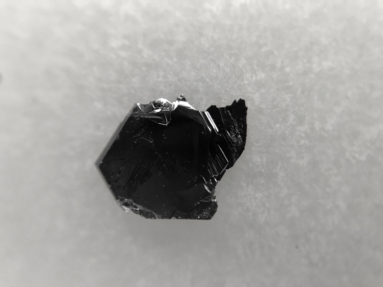
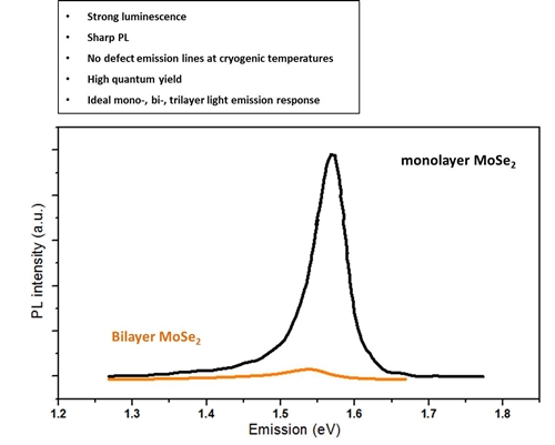
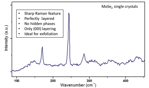
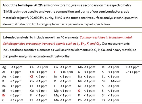
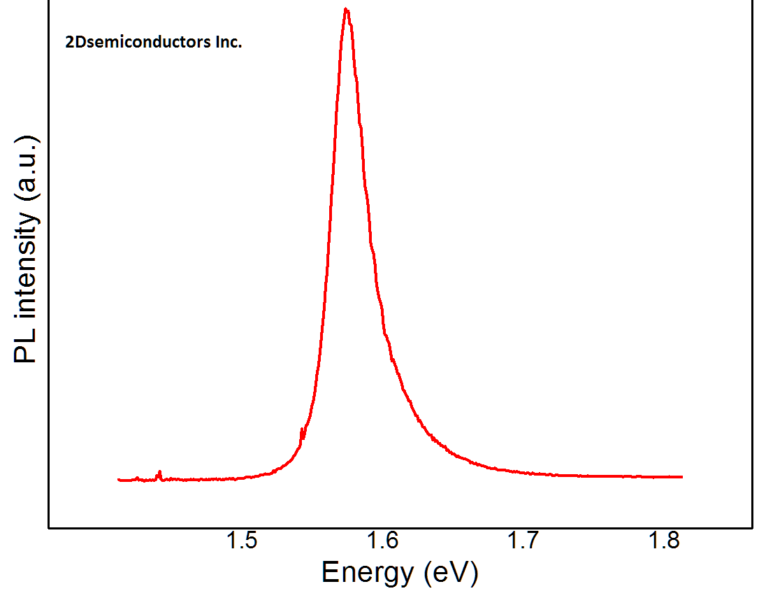
Our MoSe2 crystals are grown using two different techniques through chemical vapor transport (CVT) or flux zone growth (see description of these two methods below). These crystals are treated as gold standards in 2D materials field owing to perfected optical and electronic behavior. Our MoSe2 crystals are notoriously known to possess extremely narrow PL bandwidths, display clean PL spectra, no bound exciton shoulders at low temperatures, high carrier mobility, extremely clean and sharp XRD peaks, and negligible amount of defects (see published results as well as CVT vs. Flux based methods below ). These are the only commercially available MoSe2 crystals with guaranteed valleytronic response, sharp PL, and good electronic response.
Properties of single crystal vdW MoSe2

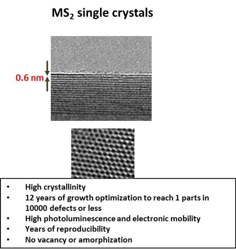
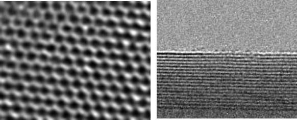
Growth method matters> Flux zone or CVT growth method? Contamination of halides and point defects in layered crystals are well known cause for their reduced electronic mobility, reduced anisotropic response, poor e-h recombination, low-PL emission, and lower optical absorption. Flux zone technique is a halide free technique used for synthesizing truly semiconductor grade vdW crystals. This method distinguishes itself from chemical vapor transport (CVT) technique in the following regard: CVT is a quick (~2 weeks) growth method but exhibits poor crystalline quality and the defect concentration reaches to 1E11 to 1E12 cm-2 range. In contrast, flux method takes long (~3 months) growth time, but ensures slow crystallization for perfect atomic structuring, and impurity free crystal growth with defect concentration as low as 1E9 - 1E10 cm-2. During check out just state which type of growth process is preferred. Unless otherwise stated, 2Dsemiconductors ships Flux zone crystals as a default choice.
http://meetings.aps.org/Meeting/MAR18/Session/K36.3
http://meetings.aps.org/Meeting/MAR17/Session/V1.14
Publications from this product
Summary: Publications from MIT, Berkeley, Stanford, Rice, and Harvard teams at top journals like Nature, Nature Communications, Nano Letters, and Advanced Materials
Control of Exciton Valley Coherence in Transition Metal Dichalcogenide Monolayers, Phys. Rev. Lett. 117, 187401 (2016)
Measurement of the optical dielectric function of monolayer transition-metal dichalcogenides: MoS2, MoSe2, WS2, and WSe2, Yilei Li, Alexey Chernikov, Xian Zhang, Albert Rigosi, Heather M. Hill, Arend M. van der Zande, Daniel A. Chenet, En-Min Shih, James Hone, and Tony F. Heinz; Phys. Rev. B 90, 205422 (2014)
Y. Jin "A Van Der Waals Homojunction: Ideal p–n Diode Behavior in MoSe2" Advanced Materials 27, 5534–5540 (2015)
Tongay et. al. "Defects activated photoluminescence in two-dimensional semiconductors: interplay between bound, charged, and free excitons" Scientific Reports 3, Article number: 2657 (2013)
M. Yankowitz et. al. "Intrinsic Disorder in Graphene on Transition Metal Dichalcogenide Heterostructures" Nano Letters, 2015, 15 (3), pp 1925–1929
Tongay et.al. Thermally Driven Crossover from Indirect toward Direct Bandgap in 2D Semiconductors: MoSe2 versus MoS2; Nano Letters, 2012, 12 (11), pp 5576–5580
Manish Chhowalla, "Two-dimensional semiconductors for transistors" Nature Reviews Materials 1, Article number: 16052 (2016) doi:10.1038/natrevmats.2016.52
X Li et al. "Determining layer number of twodimensional flakes of transition-metal dichalcogenides by the Raman intensity from substrates" Nanotechnology 27 (2016) 145704
L. Zhang. et.al. "Photonic-crystal exciton-polaritons in monolayer semiconductors" Nature Communications volume 9, Article number: 713 (2018)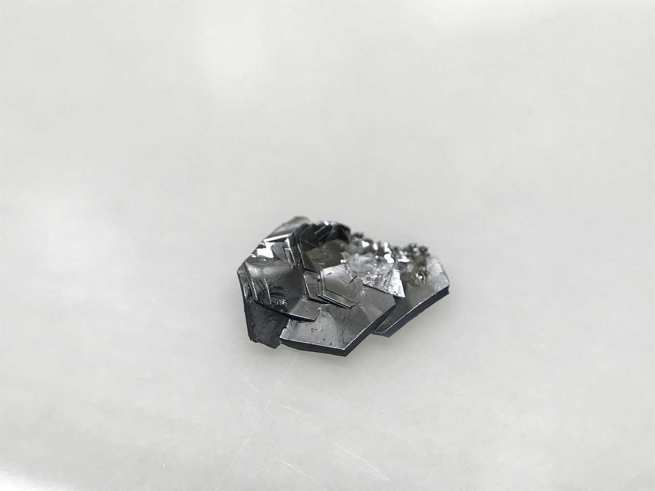
產(chǎn)品咨詢
聯(lián)系我們
上海巨納科技有限公司 公司地址:上海市虹口區(qū)寶山路778號海倫國際大廈5樓 技術(shù)支持:化工儀器網(wǎng)掃一掃 更多精彩

微信二維碼

網(wǎng)站二維碼
 歡迎來到
歡迎來到